What Is ASIC? Application-Specific Integrated Circuit vs GPU
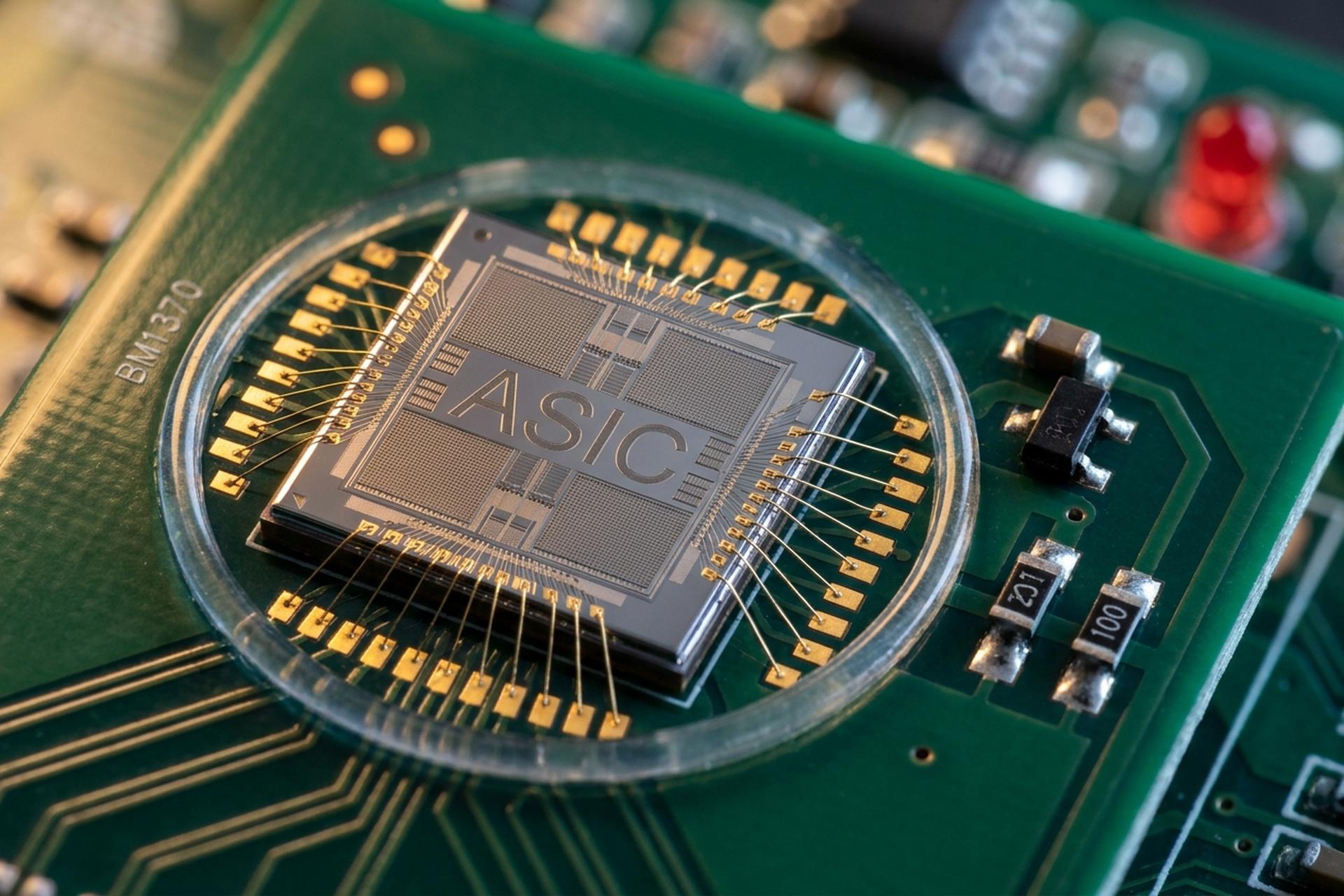
Open up a Bitcoin miner, look at the chip inside, and you are looking at silicon that does exactly one thing. It hashes. That is the entire job. It cannot run a web browser. Will never decode a Netflix stream. Will not train an AI model. But the one thing it does, it does about a thousand times more efficiently than any general-purpose chip on the market. The name for that kind of silicon is ASIC, short for Application-Specific Integrated Circuit. They turn up in plenty of places far beyond crypto too. Google's data centers. The radio modem in your phone. Tesla's autopilot computer. Every Ethernet switch in your office. This piece walks through what an ASIC actually is, how one gets designed, what makes it different from a CPU, GPU, or FPGA, why Bitcoin mining settled on ASICs by 2013, and how the 2026 generation stacks up against the latest GPUs.
What an ASIC is, in one paragraph
An ASIC is a chip built for one specific task at the highest possible energy efficiency. The acronym is Application-Specific Integrated Circuit, sometimes printed without the hyphen as application specific integrated circuit. Once the design is etched into silicon at a foundry like TSMC or Samsung, the logic cannot be reprogrammed. Every transistor sits exactly where ASIC design teams put it. Brutal flexibility traded for brutal optimization. A modern Bitcoin ASIC like the Antminer S21 Pro runs 234 trillion SHA-256 hashes per second at 15 joules per terahash, a level no CPU, GPU, or other processing units come close to. Google's TPU is an ASIC. So is the radio modem in your phone. So are the digital signal blocks that accelerate AI and machine learning inside the latest consumer electronics.
ASIC vs CPU, GPU, and FPGAs: a general-purpose tradeoff
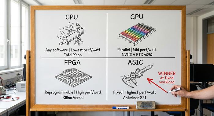
The easiest way to see what makes an ASIC different is to put it next to its alternatives. Four types of chip do most of the work in modern computing, and each one trades flexibility for efficiency in a different ratio.
A CPU (central processing unit) is the chip in a laptop. It can run any program ever written. The price is that it does no single task particularly fast per watt. A GPU (graphics processing unit) is built for parallel math. The same operation runs across thousands of small cores at once. That is great for graphics, machine learning, and ASIC-resistant cryptocurrency mining. An FPGA, short for field programmable gate arrays, is a chip whose logic gates can be reprogrammed after manufacturing using a hardware description language (HDL) such as Verilog or VHDL. FPGAs sit between GPUs and ASICs on energy efficiency, with the advantage of being reconfigurable. The cost of an ASIC at scale is far lower per chip, but the upfront NRE bill is brutal. An ASIC is the final stop. Fixed logic. Maximum perf-per-watt. No flexibility at all. Designers optimize the silicon for one workload and call it done.
| Chip type | Flexibility | Perf/watt for fixed task | Typical use | Example |
|---|---|---|---|---|
| CPU | Runs any software | Lowest | Operating systems, general code | Intel Xeon, AMD Ryzen |
| GPU | SIMD parallel, programmable | Mid | Graphics, ML training, ASIC-resistant mining | NVIDIA RTX 4090 |
| FPGA | Reprogrammable logic | High | Prototyping, telecom, HFT, low-volume custom | Xilinx Versal, Intel Agilex |
| ASIC | Fixed-function silicon | Highest | BTC mining, Google TPU, network switches | Antminer S21, Google TPU v5 |
Once you understand that table, the rest of this article is application. ASICs win when the workload is fixed, the volume is huge, and the workload has stayed the same long enough to justify a tape-out. They lose the moment the workload changes.
ASIC development: from RTL to silicon wafer
Designing an ASIC is slow, expensive, and almost entirely one-way. Six rough stages in the pipeline. Trip at any one of them, you can burn months of work and tens of millions in mask costs.
Stage one is spec and architecture. Engineers pin down what the chip must do. Performance target. Power budget. Die area. Stage two is RTL design, where engineers programme the logic at the register-transfer level in a hardware description language. Verilog and VHDL still rule. SystemVerilog has taken over verification. Stage three is functional verification itself, a mix of simulation against a testbench and formal property checking. Bugs caught at this gate cost thousands of dollars. Bugs that slip into silicon cost millions. The entire game lives here.
Stage four is logic synthesis. A compiler turns the RTL into a gate-level netlist of standard cells. Stage five is physical design. Floor-planning, placement, routing, clock-tree synthesis, timing closure. Output: a GDSII file describing every layer of the chip. Stage six is tape-out, when the GDSII goes to the foundry. Photolithographic steps then turn the design into mask sets. The masks pattern silicon wafers layer by layer. Finally the wafer gets diced into individual chips and packaged. Even the interconnect between transistors at this scale is its own research field, with PhDs written on it every year.
Now the bill. A single mask set at the 5 nm node runs $5 to $10 million. At 3 nm, $10 to $15 million or more, per Semianalysis and IBS. Add salaries, IP licenses, and verification, and the NRE bill for a leading-edge ASIC easily clears half a billion dollars. Cycle time from spec to first silicon: 12 to 24 months. Tool vendors that actually matter: Synopsys (VCS, PrimeTime), Cadence (Virtuoso), Siemens EDA. Verilog and VHDL still rule the floor after four decades. Nothing better has replaced them yet.
Types of ASICs designed: full-custom, gate-array, more
Several design methodologies sit under the ASIC umbrella. They range from painstaking full-custom work to fast pre-fabricated shortcuts.
Full-custom ASICs draw every transistor by hand. Best possible performance and density. Longest design time. Standard-cell or semi-custom ASICs use a pre-characterized library of logic gates, registers, and memory blocks. That drops development time by orders of magnitude while still hitting near-optimal results for most digital workloads. Gate-array ASICs go further: pre-fabricated wafers with unconnected transistors, where only the metal layers that wire them together are customer-specific. Cost and turnaround both fall. Structured ASICs sit between gate arrays and standard-cell, a middle path for low-volume, high-performance designs.
A little history. The bipolar gate array showed up in 1967 from Ferranti and Interdesign, with Fairchild's Micromatrix family arriving the same year. The Ferranti ULA built into the 1981 Sinclair ZX81 home computer is widely cited as the first popular consumer ASIC. CMOS gate arrays followed in 1974. Full standard-cell ASICs proliferated through the 1980s. Today's leading-edge ASICs are still descendants of that family tree.
Where ASICs are used today: TPU, networking, AI inference
ASICs are everywhere people stop looking. Open any smartphone and you find a custom application processor that is, technically, an ASIC family. Apple's A-series and M-series. Qualcomm Snapdragon. Samsung Exynos. Walk into a cloud data center and you find custom networking ASICs from Broadcom, Cisco, and Marvell, pushing terabits of traffic per second through switches that would melt if anyone tried to do the same work in software.
The most quoted modern non-crypto ASIC is Google's Tensor Processing Unit. The TPU project went from concept to deployed silicon in roughly 15 months. TPU v1 went live in Google's data centers in 2015. It was publicly disclosed at Google I/O in May 2016. A 2017 ISCA paper from Norm Jouppi's team reported TPU v1 running inference 15 to 30 times faster than the CPUs and GPUs of that era, at 30 to 80 times better performance per watt. Google is now on its eighth TPU generation, called Ironwood, aimed at the agentic AI era. The Edge TPU shipped in July 2018, bringing the same idea to low-power inference at the edge.
Automotive ASICs are everywhere too. Tesla's Dojo training chip and the FSD inference chip in its cars are both custom ASICs. Mobileye and NVIDIA ship ASIC accelerators for image processing and digital signal work in ADAS systems. Telecommunications. Autonomous vehicles. AI inference. Those are the three growth segments where ASICs are widely used and will keep dominating through the rest of the decade. ASICs cannot be reprogrammed after fabrication, so they get deployed where the workload genuinely stays put. The fourth is the one this article has been pointing toward all along: cryptocurrency mining.
ASIC miners: Bitcoin's integrated circuit story from Avalon1
Bitcoin mining is the cleanest case study of why ASICs matter at all. The Bitcoin network pays miners to compute SHA-256 hashes. SHA-256 is fixed. It has not changed since 2009. Which makes it a perfect ASIC target.
In the early years, mining ran on whatever hardware happened to be in the house. CPU mining peaked through 2009 and 2010. GPUs took over from 2010 to 2012 once people figured out that graphics cards could hash orders of magnitude faster than a Core i7. A brief FPGA window opened in 2011 and 2012 for the most committed miners. Then Canaan Creative shipped Avalon1 on January 19, 2013, the first commercially produced Bitcoin ASIC. The first unit hit 60 GH/s on 600 watts, fabbed on a 110 nm process. The entire global Bitcoin network was running about 20 TH/s at the time, which meant a single Avalon1 could mine an estimated 15 to 20 BTC per day at launch. The mining business as we know it really dates from that day.
Bitmain was founded the same year in Beijing, by Jihan Wu and Micree Zhan. MicroBT (Whatsminer brand) followed in 2016, spun out by ex-Bitmain engineer Yang Zuoxing. By the second half of 2013, GPU Bitcoin mining was already unprofitable. CPU mining had been dead for two years. Since then the only economically rational way to mine Bitcoin has been with ASICs. Period.
Consolidation has been sharp. Bitmain currently holds an estimated 82% of the global ASIC miner market. In 2024 the US slapped a 25% Section 301 tariff on Chinese-made ASIC mining hardware, which has reshaped where miners deploy fleets and where ASIC chip fabrication actually lands. The crypto end of the semiconductor business now sits squarely inside the US-China trade story.
ASIC vs GPU mining in 2026: hashrate, watts, ROI
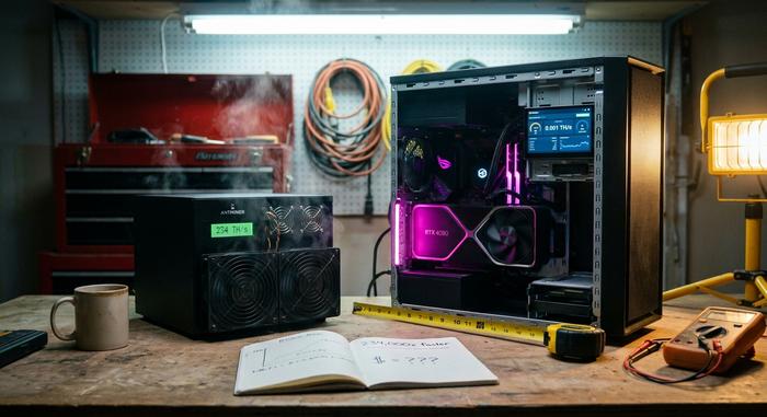
Comparing an ASIC miner to a GPU on Bitcoin in 2026 is not a contest, it is a category error. The numbers explain why.
As of May 2026, Bitcoin trades near $77,347 per coin according to Fortune's daily price tracker. Network hashrate sits at roughly 1,012 EH/s on a 7-day average, per Hashrate Index. Difficulty hovers near 136.61 T. The block reward has been 3.125 BTC since the April 19, 2024 halving. The hashprice — the revenue a miner earns per unit of hash power — stands at $39.04 per PH/s/day, which works out to about $0.039 per TH/day.
| Model | Hashrate | Efficiency | Power | Cooling | Daily revenue at $0.039/TH |
|---|---|---|---|---|---|
| Antminer S21 Pro | 234 TH/s | 15 J/TH | 3,510 W | Air | ~$9.13 |
| Antminer S21 XP Hydro | 473 TH/s | 12 J/TH | 5,676 W | Hydro | ~$18.45 |
| Whatsminer M60S++ | 226 TH/s | 15.93 J/TH | 3,600 W | Air | ~$8.81 |
| Whatsminer M63S+ | 450 TH/s | 17 J/TH | 7,650 W | Hydro | ~$17.55 |
Plug $0.07 per kWh, a common large-farm rate, and the S21 Pro draws roughly 84 kWh per day at a cost of about $5.88. Net of energy: a few dollars per day. Breakeven electricity for the S21 Pro at current hashprice lands near $0.108/kWh. The whole network draws an estimated 170 to 180 TWh per year, around 0.7 to 0.8% of global electricity according to the Cambridge Centre for Alternative Finance.
Now the GPU side. An NVIDIA RTX 4090, the top consumer card of the last generation, computes Bitcoin SHA-256 at roughly 1 to 2 GH/s. That is 0.001 to 0.002 TH/s, against the S21 Pro's 234,000 GH/s. The S21 Pro is more than 100,000 times faster than a $1,600 graphics card. It also runs at 75 dB, about the noise level of a roadside vacuum cleaner, while hydro models drop to 50 dB. For SHA-256, general-purpose chips need not apply.
GPU-mineable coins in 2026: where GPUs still beat ASICs
A handful of proof-of-work coins still keep GPUs in the game in 2026, mostly because their algorithms were built to be hostile to ASIC silicon.
Ergo runs Autolykos2, a memory-hard algorithm that has stayed GPU-only since day one. Ravencoin uses KawPow. An RTX 4090 there does about 120 MH/s. Alephium runs Blake3 and remains GPU-only in practice. Monero leans on RandomX, which is deliberately CPU-only and built around random program generation, killing any ASIC advantage. Kaspa lost its ASIC-resistance window in 2023, when IceRiver and then Bitmain shipped dedicated kHeavyHash ASICs. Ethereum Classic's Ethash has been ASIC-mined since 2018. Zcash's Equihash fell to ASICs years before that.
The pattern is consistent. Memory-hard or frequently-rotated algorithms resist ASIC takeover for years. Fixed compute-heavy algorithms always fall. That is silicon economics, nothing more.